PCB Editor
Introduction
There are many PCB editors. Large and strong teams create and maintain them. Why do we need another one?
Because it is simple.
It is probably the simplest PCB editor in the world, it took me just four days of coding.
As I am going to build robots here, "in front of your eyes" so to speak, I want it to be done right. And spagetti-wiring it is NOT a good style. Like this (though it is kind of ok for prototyping):
But to design a simple PCB, we do not need software capable of simulating components. We do not need it to comply to standards that our robot doesn't care about. We particularly do not need it to be Web-based and expensive.
So I have created a simple one. Probably, the simplest PCB editor ever. Note how I am doing my best to avoid using the term "primitive".
Installation
The PCB editor is part of an archive. Use it from there or
move its folder wherewer you want. To run it, start terminal and run
pyrtoh3 pcb_editor.py
It has, of course, dependencies. Most of them come with Ubuntu, you will need TkInter, PIL and OpenCv. To see a complete list of dependencies, look at the "import" part of a Python file pcb_editor.py. You will see something like this:
Every line is a package the script uses, however, as I mentioned, some of them are part of Ubuntu and do not need to be installed.
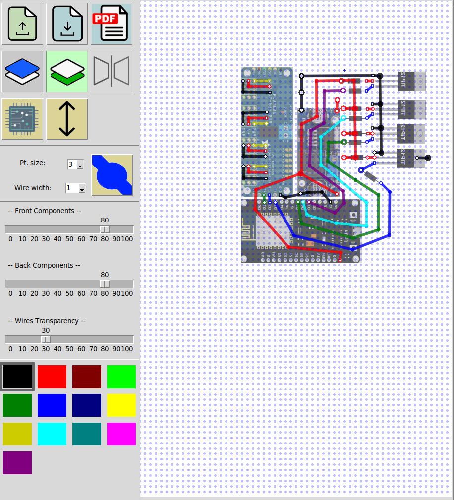
Open and save project


Switch layers


Editor has max. 2 layers (2-sided PCB), so you can switch between them. Wires on non-active layer fade to make it easier to distinguish.
Mirror

Works on components (not on wires). When component is at the opposite side of PCB, it should be mirrored, unless it is up side down. So select component and click this button.
Load component

Loads YAML file describing component. You are responsible for your components. But good news - it is very easy to make one. Find image on Google, and enter its dimensions, that's all. Dimensions are in millimeters.
Example:
Moving object between layers

Moves object (either selected component or selected wire) from front to back and from back to front.
Editing wires and components
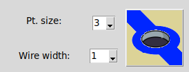
Here you can change size of end point, its type and width of the wire.
To select wire, click on one of its points (not on a connector). Make sure this wire is on the layer currently active, or selecting will not work. Shift-click outside wires to start a new one. Control-click on a point to change its type and size according to what is selected in combo boxes. Pressing Delete deletes a segment where selected point is. Control-clicking also changes color.
Control-mouse move rotates component.
Transparency
![]()
You can change transparency of front or back components. You can change transparency of wires of a non-active layer.
Export to .gcode

G-code is the format 3d printers understand. In my next post I am going to explain how to use 3d printer to draw on PCB. Using this approach we can create high quality printed boards for our robots.
Note that clicking on "Save as g-code" button only saves the current side of a design. Which is understandable, as 3d printer can only print one side of a PCB in a time. So to save 2 sides (in 2 different files) you need to select the side (front of back icon) and to repeat the saving procedure.
Printing on PCBs
Introduction
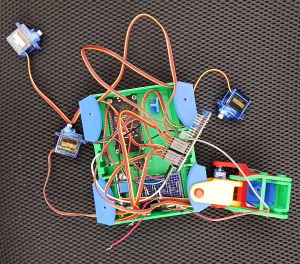
Earlier, I have presented a rather primitive PCB editor that allows you to draw very simple PCBs for your DIY robots. It can then export these PCBs to g-code files that 3d printer can understand. Now we can print these schematics on a PCB.
First of all, why do we need to print on a Printed Circuit Board? The idea is to draw our wires on a board's copper covered surface with some kind of a protective paint, and then to dissolve the areas that are not covered. Do not worry, dissolving is an easy task and i will cover it in my next post.
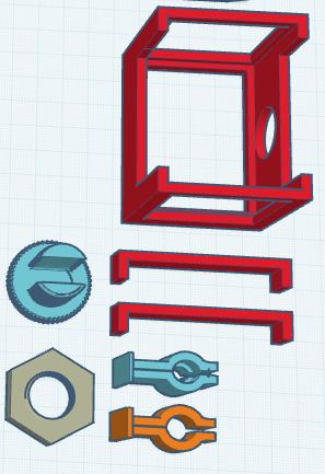
In this post I have created a simple add-on to an extruder of a 3d printer that turns it into a 2d plotter. And if your 3d printer has different extruder, you can design your own plotter head using mine as an example.


On sites like Thingiverse you can find many alternative designs. So let me stress the advantages of mine: it uses a spring. Two fragments of a credit card (debit, discount or id cards will do) is used to make sure that the marker presses firmly against the surface and in the same time, doesn't press too hard, destroying the tip. That makes this design much less sensitive to errors in vertical positioning of a pen: few millimeters up or down are not critical.
Design
It is a box that you squeeze on your extruder fan. Parts are connected using glue. The spring is made of strips of a plastic card.
Additional Considerations
The PCB editor I used is very primitive. It might or midht not change, but for now it is very limited. One of the things to keep in mind is "how do we position the pen", because obviously, the marker's tip is shifted relative to extruder's tip.
To do it, we edit the code. Yes, I understand that it should be part of UI, but it is not - yet. In a PcbEditor() class (located in bcb_editor.py), you will find the following lines:
The first two lines allow you to move the starting point of your drawing to any point on a printer's table.
Let's go over the entire printing procedure.
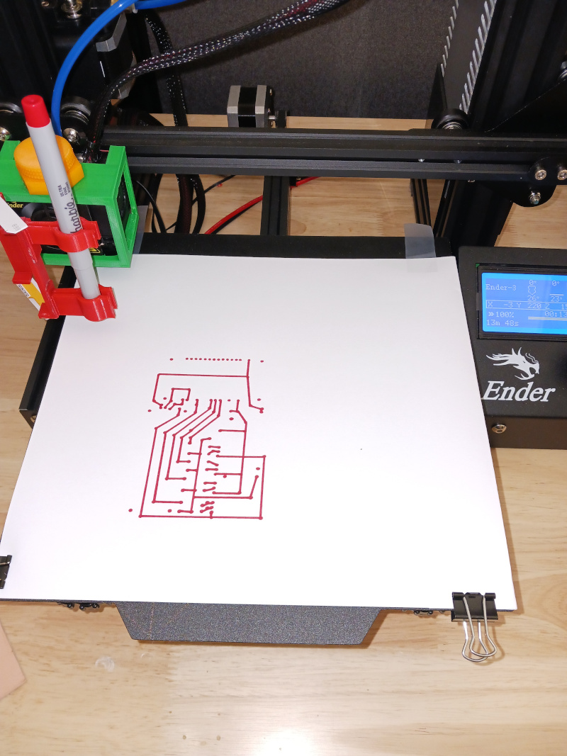
1. Put, using tape, a sheet (or few sheets) of paper on top of the printer's table. You do not want to draw on printer's table directly.
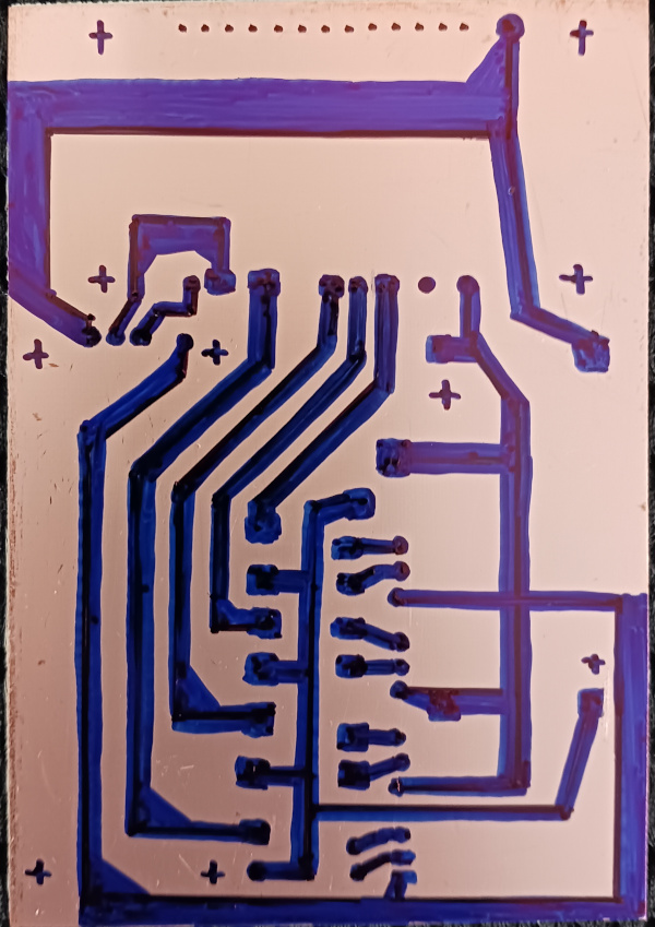
In your PCB design, draw markers at the corners of your design or a frame around it. You can see such frame on the following image:

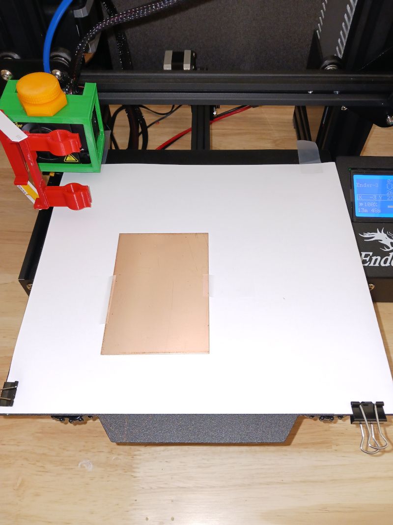
3. Attach, using tape, the PCB so that it is located properly. Make sure it covers your design that you printed on the paper.
4. Print. I use Sharpie markers with 0.2mm point size. If you use something else, you will have to redesign the pen holder. Any color will do, not just black.
Printing
First, we need to attach paper to printer's bed. By printing the PCB on this paper, we mark the area, so we know exactly where to attach the actual PCB on the next stage:
Then we attach the PCB so that it covers the printable area, right on top of what we just printed:
Next, we perform printing on PCB: note the way I used thin stripes of tape to hold it in place. Of course, there can be other options, like double-sided tape under the PCB.
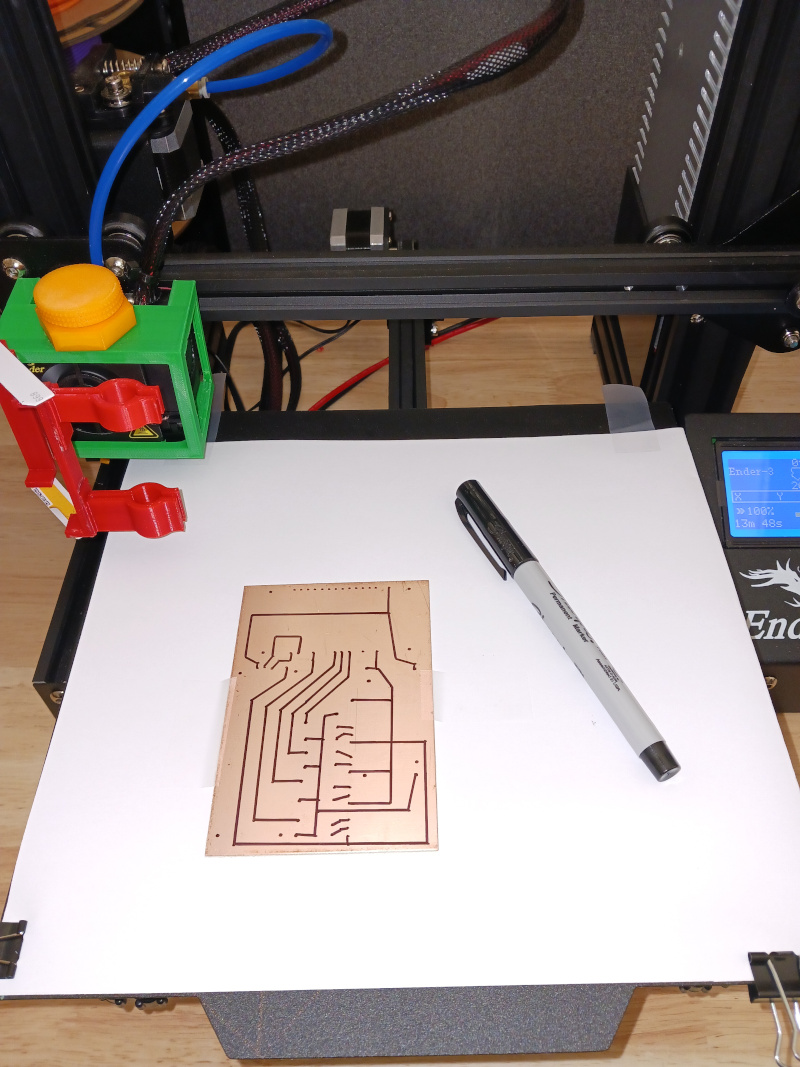
The next step is not mandatory, but I find it useful. It is possible to improve (yes, by hand) the image, making it thicker. Of course, if my PCB editor was of a pro level, that would be handled on a stage of designing. Note that I used blue marker to add changes: color doesn't really mater.